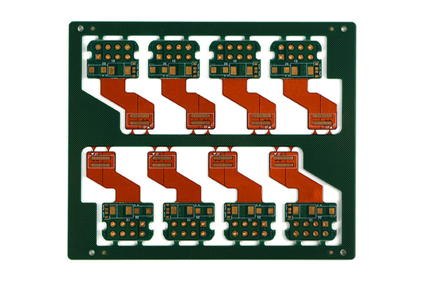
1. Cutting: Roll up flexible substrates, conductive materials, insulation materials, etc., according to the production instruction (MI) size, are processed or cut into the required size by a slitting machine or slicing machine to meet the specifications of different products.
2. Inner layer circuit production:
Graphic transfer: Transfer design graphics onto copper foil through exposure, development, and other processes. First, apply a dry film on the surface of the copper foil, then use photolithography technology to transfer the circuit pattern from the negative film to the dry film through ultraviolet exposure, and then process it with a developing solution to remove the dry part of the unexposed part
The film exposes the copper foil that needs to be etched.
Etching: Using chemical etching solution to remove excess copper foil and form inner layer circuit patterns. The etching process requires strict control of the concentration, temperature, and time of the etching solution to ensure etching accuracy and circuit accuracy.
AOI inspection: using automatic optical inspection equipment to inspect the produced inner circuit, detecting whether there are defects such as short circuits, open circuits, and abnormal line widths in the circuit.
3. Layering:
Stacking: Stack the inner circuit board and insulation layer (such as cover film, adhesive, etc.) in the order required by the design to ensure the alignment accuracy between each layer.
Hot pressing: Under high temperature and high pressure conditions, the stacked layers are combined into one, forming a multi-layer structure. During the compression process, it is necessary to control parameters such as temperature, pressure, and time to ensure a firm bond between the layers and avoid problems such as delamination and bubbles.
4. Drilling: According to design requirements, use mechanical drilling or laser drilling to drill through holes or blind holes at designated locations to achieve electrical connections between different layers. When drilling, attention should be paid to controlling the accuracy and depth of the borehole to avoid problems such as hole position deviation and rough borehole walls.
5. Hole metallization:
Chemical copper deposition: A thin layer of conductive copper is deposited on the wall of a drilled hole, and a uniform copper film is formed on the surface of the hole wall through chemical plating to achieve electrical conductivity between layers.
Electroplated copper: Electroplated copper treatment is applied to the hole walls after chemical copper deposition, thickening the copper layer on the hole walls to improve conductivity and reliability, in order to meet electrical performance requirements.
6. Outer layer circuit fabrication: Similar to the inner layer circuit fabrication process, it includes steps such as pattern transfer and etching. The outer circuit pattern is transferred onto the copper foil through processes such as film sticking, exposure, and development, and then the excess copper foil is etched away to form the outer circuit.
7. Surface treatment: Select the appropriate surface treatment process according to the product's usage requirements, such as gold plating, silver plating, tin plating, OSP (organic solder mask), etc. These treatments can improve the oxidation resistance, soldering performance, and corrosion resistance of the FPC surface.
8. Applying protective film: In order to protect the circuit board from damage, after etching and film stripping are completed, a protective film, such as a cover film, is selectively applied to the areas that need to be protected, while exposing the assembly area to prevent short circuits and oxidation of the circuit.
9. Text production: Screen printing or spray printing text and marking symbols on the board surface for easy identification, assembly, and maintenance of subsequent products.
10. Electrical testing: Use professional testing equipment, such as flying needle testing machines or ICT testing machines, to conduct electrical performance tests on FPC, detecting parameters such as circuit continuity, insulation resistance, impedance, etc., to ensure that the product meets electrical performance requirements.
11. Accessory assembly: According to customer requirements, use automated equipment to attach adhesive paper, steel sheets, electromagnetic shielding film, FP4 and other accessories to the circuit board, and ensure accurate placement of accessories through optical point positioning.
12. Molding: Use mold stamping or laser cutting to process large workboards into sizes and shapes that meet customer requirements, removing excess corner materials.
13. Quality inspection: Conduct a comprehensive quality inspection of the processed multi-layer FPC according to customer requirements and industry standards, including appearance inspection, size measurement, electrical performance testing, etc., identify defective products, and ensure that product quality meets requirements.
Packaging: Qualified FPCs are packaged according to certain packaging requirements, usually using anti-static bags, paper boxes, and other packaging materials to prevent damage during transportation and storage.


